
Personal project
Sensorless BLDC speed controller
A custom circuit board and firmware built from scratch to run an e-bike motor without external sensors.
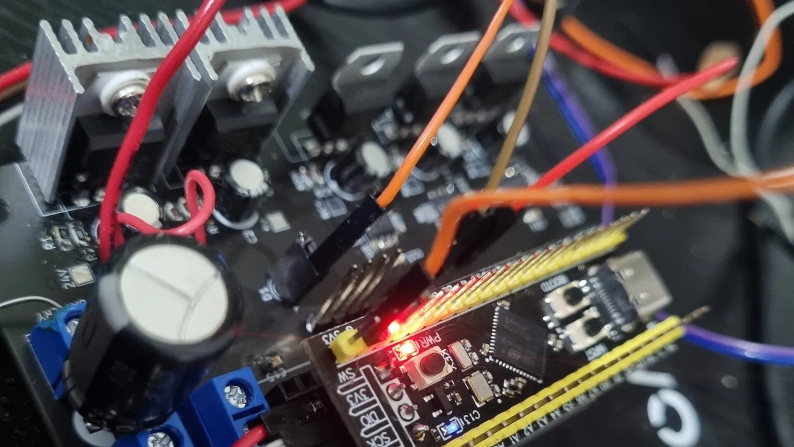
Abstract
A custom sensorless speed controller for an e-bike hub motor. The hardware and STM32 firmware execute six-step commutation on a 37 V bus using back-EMF for rotor position. The prototype successfully drove the bike and integrated throttle, brake, and lighting control. A later revision failed due to thermal overload on unprotected linear regulators.
Introduction
This project was mainly a challenge from my brother and an overly confident younger Daniel: could I develop a reliable sensorless ESC within 1 month? Although it did burn at the end, the sleepless nights and the journey taught me a lot about humility, and a bit about power electronics, embedded systems, and estimation.
No specific goal was given besides developing an ESC, but I also designed this to be suitable to fit a kit and integrate quality-of-life features like a screen, braking, and data recording, unlike most commercially available systems.
The development sections below follow the power path: power regulation, the microcontroller, the gate drivers, and the sensorless feedback loop.
Power regulation
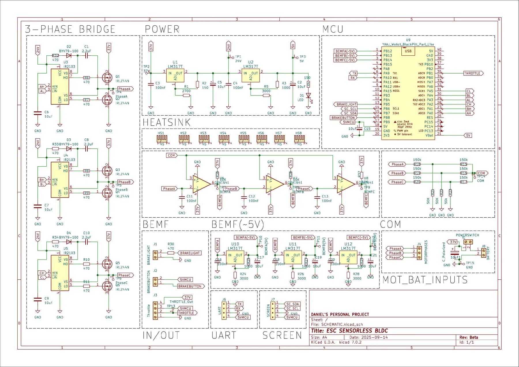
The system operates from a 37 V battery pack.
- Direct power. The pack feeds the three half-bridges directly without regulation.
- Gate drive supply. A linear regulator steps 37 V down to 24 V for the gate drivers.
- Logic supply. A second linear regulator drops the 24 V to 5 V for the microcontroller.
- Thermal cost. Linear regulators burn off excess voltage as heat rather than converting it efficiently.
The microcontroller
An STM32 module sits at the center of the board and manages all timing.
- Commutation. Six PWM lines output to the bridge, one per switch.
- User inputs. The throttle connects to an analog-to-digital (ADC) pin, and the brake to a digital input.
- Accessories. The board includes a brake light output and an I2C header for a status screen.
- Feedback. Three 5 V tolerant pins read the phase voltages for sensorless tracking.
Gate drivers and the bridge
Logic-level PWM signals cannot directly switch a MOSFET when its source floats near 37 V.
- Level shifting. Three half-bridge drivers shift the signals for each high and low MOSFET pair.
- Bootstrap circuit. Each high-side driver floats on a bootstrap capacitor, recharged through a fast diode when the low side conducts.
- Edge control. Gate resistors intentionally slow switching edges, trading minor switching losses for reduced ringing.
- Output. Six logic-level MOSFETs carry the commutated phase current out to the motor.
Feedback from the motor
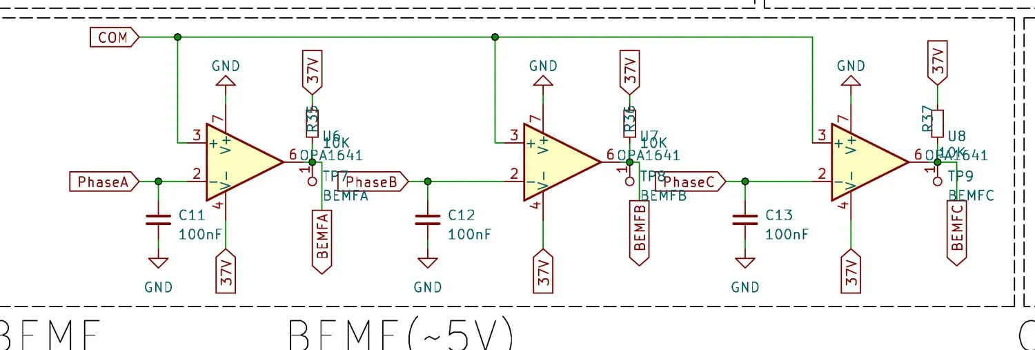
At every commutation step, one motor phase is left undriven. The spinning rotor induces a back-EMF voltage in this floating phase, providing the only position signal.
- Virtual neutral. A resistor network averages the three phases to create a neutral reference point.
- Comparators. One op-amp per phase runs open-loop, comparing the phase voltage against the neutral point.
- Scaling. The comparator outputs swing to the 37 V rail, requiring a final linear step-down before the microcontroller.
- Timing. The zero-crossing occurs exactly 30 electrical degrees before the next commutation step.One electrical turn equals one mechanical turn divided by the number of pole pairs.
Layout
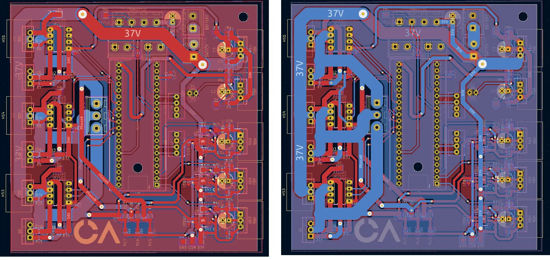
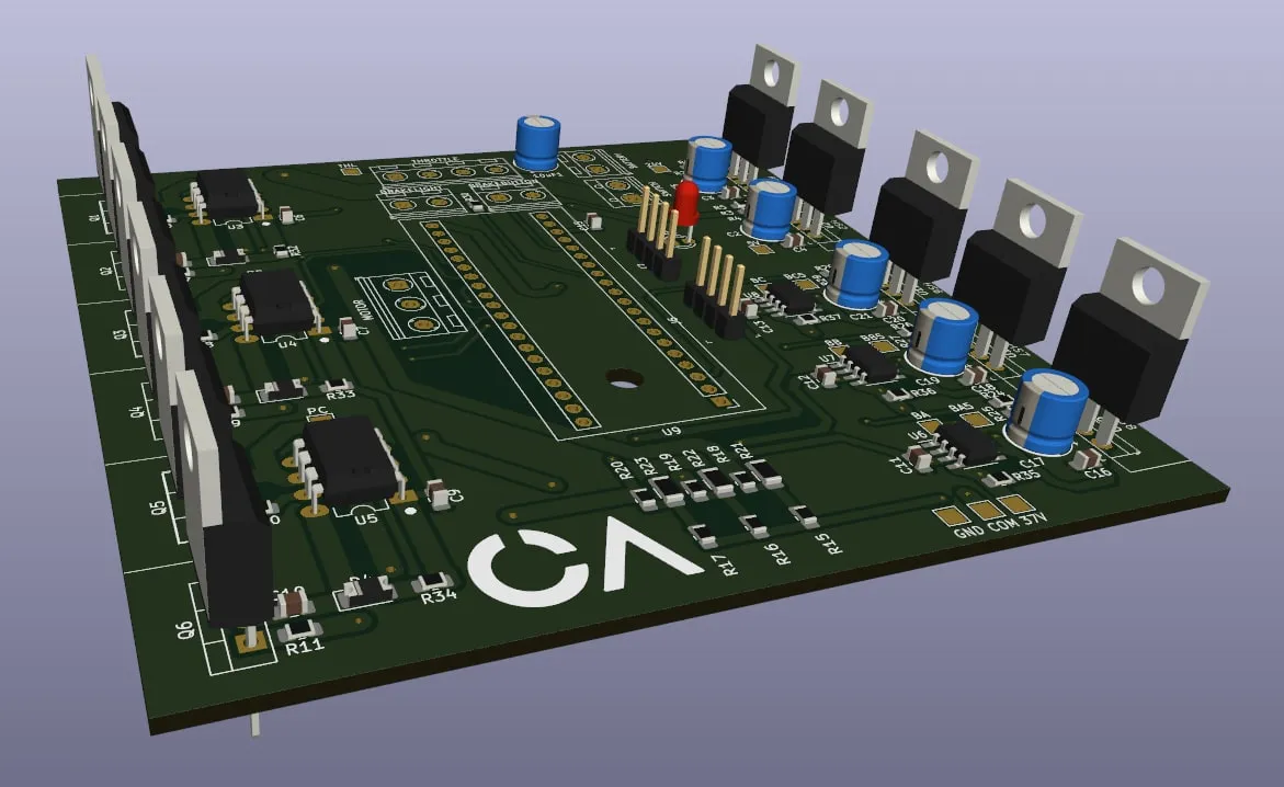
The board uses two copper layers with wide pours for the battery rail and ground. Screw terminals handle the high-current pack and phase connections. Eight heatsink footprints line the power components.
Results
The prototype motor ran smoothly. Speed control and auxiliary bike functions behaved exactly as programmed. However, during extended load testing, a board caught fire.
Limits and next steps
The primary limitation is thermal management in the power regulation stage.
- Switching regulators. Replace the linear housekeeping rails with switching converters to drastically reduce heat.
- Thermal mass. Populate heatsinks on every component that dissipates power, not just the motor bridge.
- Copper weight. Increase copper width and use proper thermal relief under hot components.